September 21, 2015 feature
Delicately opening a band gap in graphene enables high-performance transistors

(Phys.org)—Electrons can move through graphene with almost no resistance, a property that gives graphene great potential for replacing silicon in next-generation, highly efficient electronic devices. But currently it's very difficult to control the electrons moving through graphene because graphene has no band gap, which means the electrons don't need to cross any energy barrier in order to conduct electricity. As a result, the electrons are always conducting, all the time, which means that this form of graphene can't be used to build transistors because it has no "off" state. In order to control the electron movement in graphene and enable "off" states in future graphene transistors, graphene needs a non-zero band gap—an energy barrier that can prevent electrons from conducting electricity when desired, making graphene a semiconductor instead of a full conductor.
In a new study, scientists have opened a band gap in graphene by carefully doping both sides of bilayer graphene in a way that avoids creating disorder in the graphene structure. Delicately opening up a band gap in graphene in this way enabled the researchers to fabricate a graphene-based memory transistor with the highest initial program/erase current ratio reported to date for a graphene transistor (34.5 compared to 4), along with the highest on/off ratio for a device of its kind (76.1 compared to 26), while maintaining graphene's naturally high electron mobility (3100 cm2/V·s).
The researchers, led by Professor Young Hee Lee at Sungkyunkwan University and the Institute for Basic Science in Suwon, South Korea, have published their paper on the new method for opening up a band gap in graphene in a recent issue of ACS Nano.
"We successfully demonstrated a graphene transistor with a high on/off ratio and mobility by chemical methods and showed its feasibility as a memory application with a significantly improved program/erase current ratio," first author Si Young Lee, at the Institute for Basic Science and Harvard University, told Phys.org.

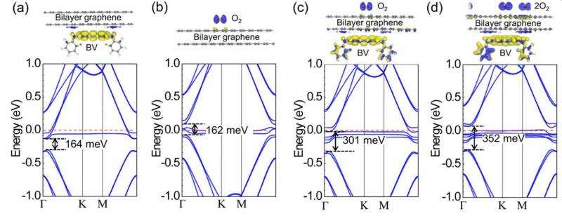
Their method is based on applying a vertical electric field through the bilayer graphene, which has been shown to break the symmetry between the two graphene layers. This modification creates atomic sites with different electric potentials, which produces a band gap. Previous studies have also used this strategy, in which the electric field is generated by "dual-side doping" of opposite sides of the bilayer with different chemicals. However, the previous results have been limited due to ineffective types and levels of dopants, which have generated relatively small electric fields and have also damaged the highly ordered graphene structure.
In the new study, the researchers demonstrate that one key to improving these areas is the choice of benzyl viologen (BV) as an electron-donating (n-type) dopant at the bottom of the bilayer graphene. The top side is then doped simply with oxygen and moisture from the atmosphere, which act as electron-withdrawing (p-type) dopants. As the BV molecules donate electrons to the bottom graphene layer, the atmospheric dopants withdraw the electrons from the top graphene layer, generating a vertical electric field.
Since a stronger electric field induces a larger band gap, the researchers could control the band gap by using higher concentrations of dopants. All of the dopants used here are absorbed on the surface of the bilayer graphene without damaging the graphene structure, which helps to maintain graphene's high electron mobility and corresponding high "on" current.
To demonstrate the usefulness of the band-gap-opened graphene, the researchers fabricated a transistor with memory behavior. The device is programmed and erased by applying a positive and negative voltage, respectively. The transistor's high program/erase current ratio corresponds to a longer retention time. However, the researchers note that the device still has room for improvement. For example, its speed can be increased. Also, using atmospheric molecules as dopants is not ideal for industrial-scale manufacturing due to low stability, so a more durable p-doping method will be needed.
"It is necessary to develop more stable and effective dopants for higher device performances," Si Young Lee said. "Furthermore, our device can be realized on flexible and transparent substrates for future electronics."
More information: Si Young Lee, et al. "Chemically Modulated Band gap in Bilayer Graphene Memory Transistors with High On/Off Ratio." ACS Nano. DOI: 10.1021/acsnano.5b03130
Journal information: ACS Nano
© 2015 Phys.org


.jpg)


