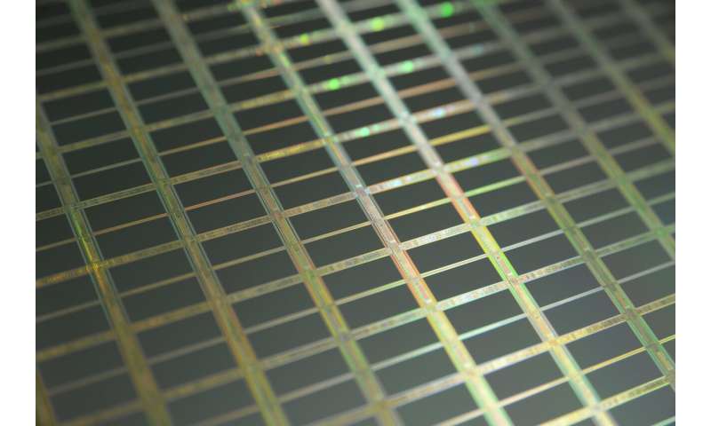
Cubic GaN on large-area silicon (100) dies

Gallium Nitride (GaN) and its alloys (i.e., III-nitride semiconductors) are the backbones of solid-state lighting, and the next-generation RF and power electronics. Today, most research and development in this material system are focused on its conventional, hexagonal (i.e., wurtzite) phase although its cubic (i.e., zincblende) phase has more inherent advantages such as: No polarization in the <100> growth direction, smaller bandgap, smaller electron-heavy hole effective masses, smaller Auger loss, larger optical gain, shorter radiative recombination lifetime, lower p-doping activation energy, higher hole mobility, and larger conduction band offset. Cubic III-nitride semiconductors might thus enable next-generation devices such as efficiency-droop-free III-nitride visible light-emitting diodes (LEDs) and as-grown, normally-off AlGaN/GaN power transistors. However, the synthesis of cubic GaN has not been an easy task due to its metastability.
In Applied Physics Letters, the U of I team reports a III-nitride materials breakthrough: The synthesis of low-defect density, stable, and pure-phase cubic GaN on the scalable Si platform. They study the structural and optical properties and demonstrate through temperature-dependent, and time resolved photoluminescence measurements the high internal quantum efficiency of ~26%. They further identify the optical defect levels and report a selective etching technique, where they can remove hexagonal GaN selectively, not only increasing the efficiency to ~32% but also pointing to the potential path of achieving a continuous cubic GaN film. Overall, U of I demonstrates an encouraging stepping stone for creating the next generation, cubic-phase-based, III-nitride devices.
More information:
J. Lee et al, Structural and optical properties of cubic GaN on U-grooved Si (100), Applied Physics Letters (2022). DOI: 10.1063/5.0102026
Provided by University of Illinois at Urbana-Champaign