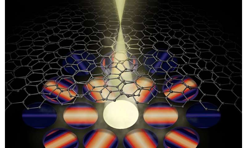
Probing the intricate structures of 2D Materials at the nanoscale

Two-dimensional (2-D) materials are just a single or a few layers of atoms thick. These materials often have exotic properties that may be useful for next-generation technologies. When layers of these materials are stacked, the electronic properties that emerge can be manipulated by, for example, twisting the layers with respect to one another. To fully understand these properties and correlate them with the twist angle, scientists need advanced microscopy techniques. Researchers developed a novel operating mode for the interferometric four-dimensional scanning transmission electron microscopy (4-D-STEM) technique. This special technique allows researchers to measure the atomic-scale structural distortions, twist angle, and interlayer spacings that influence the unique electronic properties of layered 2-D materials.
The Impact
Layered 2-D materials have special properties that can advance technology beyond existing capabilities. For example, they could lead to faster and more energy efficient computers or more reliable electricity storage. The individual layers that make up these materials may each be oriented differently. This creates challenges in fully understanding their 3-D atomic structures with existing microscopy techniques. Interferometric 4-D-STEM can reveal the relative positions of atoms within separate layers of stacked and twisted 2-D materials. The technique opens avenues to the design and development of materials with useful properties.
Summary
Layered 2-D materials have attracted considerable attention due to their interesting electronic properties, which can be modified by changing the twist angle of bilayer materials, the stacking sequence of trilayer materials, or other factors. To fully understand and control the properties of these materials, researchers need to study their atomic structures. However, visualizing the atomic structure of few-layered materials is often challenging using conventional microscopy techniques, such as when working with materials composed of light elements or when 3-D information is needed. Researchers need new techniques to improve precision and locally measure distortions and interlayer spacings in twisted materials composed of two or three layers, especially when they contain light elements or high twist angles.
Researchers developed a new interferometric 4-D-STEM modality that can provide information about local structural deformations within layers, twist direction and magnitude between layers, and interlayer distances for few-layered 2-D materials. This new operating mode of 4-D-STEM is still based on Bragg interferometry but uses a defocused electron probe to directly provide information about the relative positions of atoms within separate layers, as demonstrated in this study in bilayer and trilayer graphene. The technique sheds new light on the interplay between electronic properties and the precise structural arrangements of few-layer 2-D materials.
More information:
Michael J. Zachman et al, Interferometric 4D‐STEM for Lattice Distortion and Interlayer Spacing Measurements of Bilayer and Trilayer 2D Materials, Small (2021). DOI: 10.1002/smll.202100388
Provided by US Department of Energy