Ultrathin Sn-doped Ga2O3 for power field-effect transistors

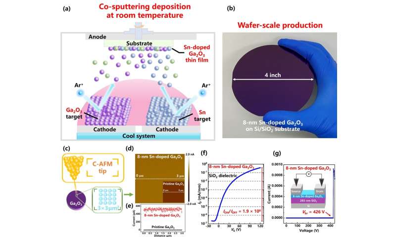
Herein, wafer-scale 8-nm films of Sn-doped gallium oxide (Ga2O3) were fabricated via physical vapor deposition at room temperature. Using these films, 8-nm Sn-doped Ga2O3 field-effect transistors (FETs) featuring SiO2 gate dielectrics were fabricated. These FETs exhibited a high on-state current of 3.8 × 10⁻¹ mA/mm and a high on/off ratio of 1.9 × 10⁶.
Notably, they also demonstrated a high breakdown voltage of over 400 V, showcasing their potential for power nanodevices. Even after exposure to air for a year, these FETs maintained their normal electrical characteristics, withstanding a ± 100 V gate-bias stress for 1 hour while retaining a breakdown voltage of over 400 V, underscoring their strong endurance capability.
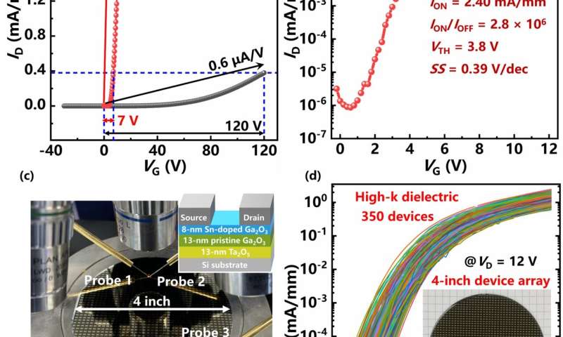
Moreover, their performance was enhanced by replacing the traditional SiO2 gate dielectric with a high-k bilayer comprising Ta2O5 and pristine Ga2O3. This modification reduced subthreshold swing and threshold voltage, enabling high-speed operation and low power consumption. Moreover, a 4-inch 8-nm Sn-doped Ga2O3 FET array was successfully fabricated on a 4-inch silicon substrate, employing the high-k Ta2O5/pristine Ga2O3 gate dielectric.
Averaged 350 devices in the 4-inch array, a low driving voltage with a small threshold voltage of 4.1 V is achieved to drive a high on-state current of 1.3 mA/mm. This study provides a promising, efficient, and economical method for producing wafer-scale ultrawide-bandgap semiconductor Ga2O3 device array and enabling their heterogeneous integration with silicon, paving the way for future Si-compatible power nanodevices.
The work is published in the journal Science Bulletin.

More information:
Zi-Chun Liu et al, Ultrathin Sn-doped Ga2O3 for power field-effect transistors: Si-compatible 4-inch array with high-k gate dielectric, Science Bulletin (2024). DOI: 10.1016/j.scib.2024.04.059
Provided by Science China Press