Entering the High NA EUV Lithography era

Preparing High NA EUV for high-volume manufacturing
Steven Scheer: "The opening of the joint ASML-imec High NA EUV Lithography Lab in Veldhoven, the Netherlands, marked a milestone in preparing High NA EUV for adoption in mass manufacturing [1]. Leading-edge memory and logic chip manufacturers have now access to the first prototype High NA (0.55NA) EUV scanner (the TWINSCAN EXE:5000) and surrounding infrastructure—including a coat and development track, metrology tools, and wafer and mask handling systems. Imec and ASML will support the IDMs and foundries in de-risking the patterning technology and in developing private High NA EUV use cases before the scanners are operational in their production fabs.
Access will also be provided to the broader ecosystem of suppliers. The development facility will enable them to be at the forefront of engineering High NA EUV specific materials and equipment. A third group of users are imec and several of our partners in the advanced patterning program, driving the patterning ecosystem into the next generations of High NA EUV.
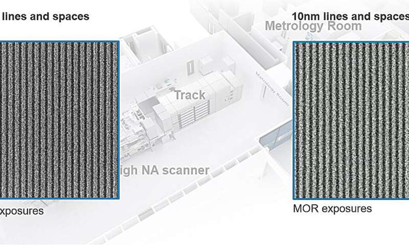
The joint High NA EUV Lithography Lab in Veldhoven was established to bring High NA EUV into production in an accelerated and cost-efficient manner. In a short period of time, ASML and ZEISS have developed High NA EUV scanner specific solutions related to the source, optics, lens anamorphicity, stitching, reduced depth of focus (DOF), edge placement errors (EPE) and overlay accuracy. In parallel, imec, in tight collaboration with ASML and our extended supplier network, readied the 0.55NA patterning ecosystem—as announced at the 2024 SPIE Advanced Lithography and Patterning Conference [2]. We ensured the timely availability of advanced resist and underlayer materials, photomasks, metrology techniques, (anamorphic) imaging strategies, optical proximity correction (OPC), and integrated patterning and etch techniques for the first generation of High NA EUV. All the preparatory work recently resulted in exposure of the first wafers. 10nm and 16nm wide lines/spaces (i.e., 20nm and 32nm pitch) could successfully be printed after exposing metal-oxide resists (MORs) and chemically amplified resists (CARs), respectively. Now the prototype scanner and infrastructure are ready, insertion in high-volume manufacturing is expected in the 2025-2026 timeframe."
(Figure 1—The EXE:5000 High NA EUV scanner in the High NA Lab demonstrating 16nm lines and the first-ever 10nm dense lines obtained in a single exposure.)
First use cases: 14A logic chips and D0a DRAM
"High NA EUV will be first introduced in the mass manufacturing of logic chips of the 14A generation, where it will enable the patterning of metal lines/spaces (M0/M2) with 24nm pitch in one single exposure, ultimately targeting 18nm pitch. This will improve yield and reduce cycle time, and may even reduce CO2 emissions compared to existing multi-patterning 0.33NA EUV schemes. It will eventually become a crucial technology for patterning the complex structures specific to complementary FET (CFET)-based chips.
Insertion in memory chip manufacturing will follow later in time for patterning the most critical structures of DRAM memories. High NA EUV is projected to image storage node landing pads and bit line periphery in one single exposure. The D0a 2D-DRAM technology generation will be the first opportunity, requiring 28nm center-to-center pitches."
Towards next generations of High NA EUV
"While the leading-edge semiconductor ecosystem targets short-term introduction of High NA EUV in high-volume manufacturing, imec and its partners take a longer-term view—aiming at enabling next generations of High NA EUV. For these activities, the joint ASML-imec High NA EUV Lithography Lab will act as a virtual extension of the imec facilities. While exposures will be carried out in Veldhoven, part of the pre- and post-processing work will continue to proceed in imec's 300mm cleanroom.
First, we will closely monitor the performance of the High NA EUV prototype litho cluster—i.e., the linked scanner and track. For that, dedicated wafer stacks have been prepared at imec and baseline processes have been transferred to the prototype High NA EUV cluster. Our team will evaluate the cluster in terms of ultimate resolution (eventually targeting 18nm metal pitch for lines/spaces, and 28nm pitch for contact holes), stability (for example, stability of the critical dimension (CD) and defect density of the structures after exposure), and effective depth of focus (DOF). Because of the larger numerical aperture, the DOF is expected to be 2-3 times smaller compared to 0.33NA EUV—one of the reasons for using thinner resist films in 0.55NA EUV.
In addition, together with our partners in metrology, we have developed and installed dedicated inspection tools in the joint Lab to monitor and improve defectivity of the patterned structures. E-beam inspection has been selected as the primary tool to investigate defectivity of ultrasmall contact holes. We aim to meet the industry's ambitious goal of achieving one defect per contact hole out of one million contact holes measured. For metal lines/spaces, optical inspection tools are combined with e-beam to detect and classify defects and provide direction to achieve less than one defect per cm3.
Finally, logic and DRAM use cases are under preparation. Larger process modules will be examined in terms of patterning resolution and defectivity, using for example a combination of inspection tools and electrical testing."
Extending 0.33NA EUV activities to the benefit of both low and High NA EUV
"The latest generation 0.33NA EUV scanners in our cleanroom remain a complementary toolset to help improving the patterning ecosystem for the next generations of High NA EUV. In addition, not all chip features require High NA EUV—think of the patterning of intermediate and global on-chip interconnect lines. We therefore continue to improve the ecosystem for 0.33NA EUV as well. In addition, some of the challenges—such as the need for improved resists—are common to 0.33 and 0.55NA.

One of the focus areas of our '0.33NA extension activities' is field stitching for High NA EUV. The need for field stitching results from introducing an anamorphic lens (i.e., a lens with different de-magnification in the x and y directions) in combination with an unchanged mask blank size (allowing only half field size on the wafer). At the 2024 SPIE Advanced Litho + Patterning Conference, imec shared its latest insights in enabling at-resolution field stitching, which reduces the need for design changes to cope with the field size reduction [2]. The work was carried out on the NXE:3400C scanner in imec's cleanroom, in collaboration with ASML and our mask partners.
Another key topic is photoresist and underlayer development. Together with our resist suppliers, we are screening alternative resist materials, and benchmark their performance in terms of defectivity, roughness and dose reduction. Chemically amplified resists (CARs) have dominated the field of optical lithography for decades and will continue to do so for selected use cases. But High NA EUV may mark a breakthrough for metal-oxide resists (MORs), who have shown good performance for high-resolution lines/spaces and small hexagonal pillars. Fundamental investigations of how these MORs react with EUV light will allow us to overcome the remaining challenges, such as their stability in performance. We also investigate underlayer matching with the resists to improve their adhesion. In addition, selection of the underlayer and resist material combination provides a knob to further reduce exposure dose, which leads to (High NA) EUV cost reduction.
Finally, we focus on directed self-assembly (DSA), which uses the micro separation of a block copolymer (BCP) to define a pattern. Industry has taken an interest in using DSA in combination with EUV because of its ability to reduce roughness, heal defects and lower the EUV dose. Our aim is to further reduce defectivity within DSA patterns. On the longer term, we will extend our DSA developments towards High NA EUV. To be relevant for High NA EUV, we will have to scale DSA patterns to below 24nm pitch. As this cannot be achieved with the currently used PS-b-PMMA-type of block copolymers, we have initiated research into so-called high-χ BCPs—together with our DSA material suppliers."
Hyper-NA EUV: the next highlight in photolithography?
"Although it's way too early to call it the next highlight, imec and ASML have started feasibility studies of Hyper-NA EUV. With an even higher NA of 0.75-0.85, Hyper-NA may become the successor of 0.55NA EUV, allowing the industry to print lines/spaces with pitches far below 20nm—as such avoiding falling back on High NA EUV multi-patterning.
Whether this technology will become reality will depend on industry demand, and on the ability to overcome technological stumbling blocks. Imec, for example, is investigating through simulations the imaging feasibility of using Hyper-NA EUV. One of the issues is the further reduction of the DOF, which shrinks inversely proportional to the square of the NA. Is the total available DOF still workable for the industry, and how can we deal with these constrained DOF resources? But in the end, as with previous generations of optical lithography, the decision will also be guided by the extent to which the costs can be reduced. It's about finding the economic sweet spot – the point in time when the costs and benefits of introducing the new technology begin to outweigh the increasing challenges associated with the 'older' one."
Reducing the CO2 equivalent footprint
"We used our virtual fab model, imec.netzero, to quantify the environmental impact of transitioning from low-NA EUV multi-patterning to High NA EUV single exposure. A major source of CO2 emissions is the electricity consumption during the lithography step. Our model shows that, in a single lithography step, a 0.55NA EXE:5200 scanner consumes more power than a 0.33NA NXE:3800 scanner—assuming the same EUV light source and wafer throughput. This is mainly due to faster wafer and reticle stages required to maintain throughput with the smaller scan lengths associated with High NA EUV. The limited scan is a consequence of the anamorphic lens used for the larger NA.
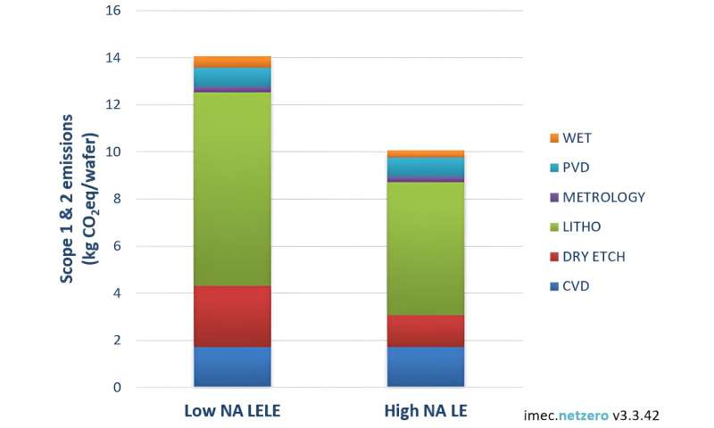
Despite the higher power consumption of the High NA scanner, our model shows an overall 30% reduction of CO2 emissions when replacing one EUV low-NA litho-etch-litho-etch (LELE) via process module with a High NA single exposure equivalent [3]. Process simplification outweighs the increase in power consumption associated with stage acceleration. Electricity consumption can be controlled by maximizing the scanner throughput, which is measured in wafers per hour (wph). Lowering photoresist dose and managing die size/reticle layout have been identified as key knobs to maintaining that throughput, as they both impact the time needed by the High NA EUV scanner to complete the wafer exposure.
(Figure 2—Graph showing 30% reduction of CO2 equivalent emissions when replacing low-NA LELE by High NA single exposure. A nominal 220wph throughput is assumed in both cases.)
In addition to lithography, etch processes contribute significantly to direct CO2 emissions. Most dry etch processes rely on fluorinated compounds that have much higher global warming potential than CO2. We develop processes and design directions to reduce the release of these fluorinated compounds.
There are other areas of concern beyond emissions, such as material scarcity and the use of toxic substances such as PFAS. PFAS is an intrinsic enabler of multiple aspects of semiconductor manufacturing including CARs and rinse materials. High NA EUV may mark the introduction of MORs, which do not contain PFAS. We recently demonstrated good performance for patterning small lines/spaces in thin MOR resists, and for patterning contact holes using MOR resists with a binary bright field mask. But CARs will remain the workhorse for patterning less critical chip features. Together with our supplier community, we have initiated new research initiatives to explore PFAS-free or -limited alternatives and benchmark their performance."
Want to know more?
[1] 'Imec and ASML open joint High NA EUV Lithography Lab offering an early development platform to the leading-edge semiconductor ecosystem', imec press release, June 2024;
[2] 'Imec demonstrates readiness of the High-NA EUV patterning ecosystem', imec press release, February 2024;
[3] 'Imec presents levers to reduce the CO2 equivalent footprint of lithography and etch for advanced technology nodes', imec press release, February 2024.
More information:
- www.imec-int.com/en/press/asml … development-platform
- www.imec-int.com/en/press/imec … patterning-ecosystem
- www.imec-int.com/en/press/imec … -advanced-technology
Provided by IMEC