2-D or not 2-D: Scientists revise a longstanding paradigm on the physics of layered materials

Crystals only one atom thick are commonly obtained by starting with layered materials, where thousands of individual atomic planes are stacked together by weak van der Waals interactions. Scientists have spent many decades investigating layered crystals, motivated by the emergence of surprising quantum properties such as superconductivity, strong electronic correlations, and charge density waves. They have concluded that in these materials, electrons are confined within each individual atomic plane, living in a two-dimensional world, and rarely venturing along the third dimension.
This scientific paradigm stood for more than 40 years.
Due to their exceptional electronic conduction and optical properties, this class of 2-D materials is expected to revolutionize the field of optoelectronic devices. This field started with the pioneering work on graphene, research that was awarded the Nobel Prize in physics in 2010. Since then, the field has grown, thanks to the plentiful variety of accessible materials, the easy fabrication of electronic devices, and the ability to combine different layers into artificial materials with tailored properties. Thanks to advanced microfabrication technologies based on focused ion beams and the precise characterization of the material using synchrotron radiation facilities, we have challenged this longstanding belief.
In our work, published in the open-access Nature partner journal 2-D Materials and Applications, we investigated the complex and much-debated layered-transition metal dichalcogenide 1T-TaS2. This compound fascinated scientists because it collects an extremely rich variety of electronic phases, the perfect playground for physicists. In particular, its properties are strongly influenced by the appearance of "stars" made by small clusters of 13 atoms that self-organize within the weakly bounded atomic planes.
. Credit: <i>npj 2D Materials and Applications</i> (2020). DOI: 10.1038/s41699-020-0145-z")
By measuring the flow of electrical current along both and perpendicular to the atomic planes, we came to a surprising result. In certain conditions, the electrons largely prefer to jump between different atomic planes, rather than moving within them. This result is stunning, and in stark contrast to previously published research that suggested the electron motion is 1,000 times better along the planes. This great contrast of results comes from a new and more precise experimental procedure developed in close collaboration between the Laboratory of Physics of Complex Matter at EPFL, and the Laboratory of Quantum Matter at Max Planck Dresden and EPFL. To further confirm the validity of our new results, we supplemented the experiments with finite element simulations to ensure that no room for doubt remained; that electrons do, indeed, prefer to move perpendicularly to the atomic planes.
-
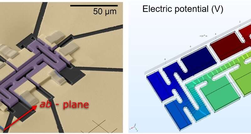
On the left, the image of the microstructured sample created by researchers at EPFL, to measure with extreme precision the conduction properties of a layered single crystal of 1T-TaS2, coloured in purple. The arrows indicate the crystal’s orientation, with the atomic layer along the ab-plane. The left image shows the result of the finite elements simulations to analyse the electric potential distribution, and validate the surprising results observed. Credit: npj 2D Materials and Applications (2020). DOI: 10.1038/s41699-020-0145-z -

Edoardo Martino (left) and Konstantin Semeniuk (right) are the two EPFL scientists who led and coordinated the project.
The surprising nature of electron motion in 1T-TaS2 is understood to originate from the characteristic orbital order within this material. The electrons follow the path defined by the overlap of each individual atomic orbital inside the crystalline lattice. For this specific compound, electrons move along the so called dz2 orbitals that belong to the Ta atoms. These orbitals have a characteristic shape of two lobes extending in opposite directions. Inside the crystal structure of 1T-TaS2, the lobes extend perpendicularly to the layers, helping electrons move more easily between then.
This new evidence is of relevance for scientists, as it is a strong argument for revising the understanding of complex properties observed in this material, above all the sudden transformation into an enigmatic electrically insulating state at low temperatures. All previous theories that described this material's electronic properties were based on the assumption that electrons live in a 2-D world, and have little interaction with those in neighbouring layers. This new discovery now supports the emergence of new theories that consider the role of interaction between separated layers.
This story is part of Science X Dialog, where researchers can report findings from their published research articles. Visit this page for information about ScienceX Dialog and how to participate.