Electromagnetic-circuit co-design approach leads to dynamically programmable holographic terahertz metasurfaces

With the help of integrated CMOS technology and electromagnetic design, Princeton researchers have demonstrated a key device that could potentially enable high-speed wireless links at terahertz frequencies.
Metasurfaces, which consist of arrays of subwavelength scatterers, can be used to precisely control incident electromagnetic fields, but are typically static once fabricated. With the use of integrated circuits, these meta-elements can be actively reconfigured at extremely high speeds. This enables dynamic control of incident electromagnetic energy. The demonstrated metasurface operates at terahertz frequencies—the frequency range between microwaves and infrared light. With the advent of 5G and Internet of Things systems, there is a growing need for high-speed data bandwidth. The terahertz band easily paves way towards high-speed data links and such devices could potentially enable many such applications. Dynamically programmable metasurfaces could either modulate the incoming beam and/or redirect the energy to a specific direction (beam-steering).
In a study published December 14 in Nature Electronics, researchers from Princeton University described the design and characterization of a CMOS-based, dynamically programmable terahertz metasurface. Design approach of the demonstrated terahertz metasurface relies on combining electromagnetic design of the surface with circuit elements, which provides an unique handle to dynamically program and engineer the incident wavefronts. The array of unit cells and integrated control circuitry can be seamlessly co-designed and integrated on a silicon wafer due to the wavelength scales and dimensions involved at terahertz frequencies.
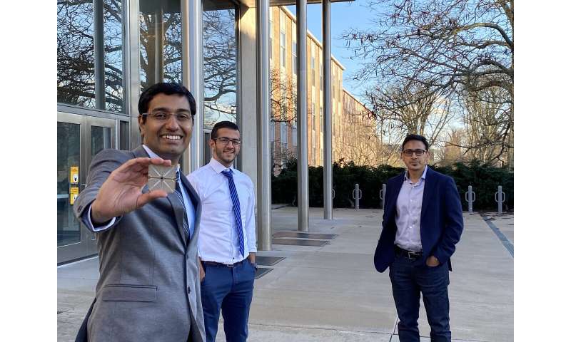
Researchers used an industry-standard CMOS process to fabricate these metasurfaces. Each integrated chip consists of 12-by-12 array of meta-elements, or unit cells, which are individually controllable through on-chip, back-end circuitry. Such integrated chips act as LEGO bricks that can be tiled together to form a larger metasurface aperture. In this study, researchers tiled 2-by-2 integrated chips to show such scalability with an overall of 576 meta-elements that are individually addressable and controllable to manipulate both the amplitude and phase of the incident terahertz beam.
"CMOS-based tiling and a scalable approach was demonstrated in this prototype, and such a design approach opens up a new architectural paradigm in the design and control of electromagnetic fields," said the lead author of article, Dr. Suresh Venkatesh, postdoctoral scholar at Electrical Engineering Department, Princeton University.

Daniel Mittleman, a professor of engineering at Brown University who was not involved in the study, commented that the research represents a significant step toward terahertz communications. "This new work demonstrates a fascinating approach which, unlike most previous efforts, is scalable into the terahertz range," said Mittleman. "The key takeaway is that we are now getting a handle on practical methods for actively controlling the wave front, beam size, beam direction, and other features of terahertz beams."
Such metasurfaces open up numerous other applications such as high-resolution imaging, gesture recognition, automotive radar, and high-speed links for augmented reality. "Looking ahead, the programmable metasurfaces will need further development to be integrated as components in innovative, next-generation networks," said Kaushik Sengupta, co-author of this work and associate professor at EE Department, Princeton University.
This work was conducted by Suresh Venkatesh (Postdoctoral Scholar), Xuyang Lu (Graduate Student), Hooman Saeidi (Graduate Student), and Kaushik Sengupta (Associate Professor) at Princeton University. The work was supported in part by the Office of Naval Research, the Air Force Office of Scientific Research, and the Army Research Office.
This story is part of Science X Dialog, where researchers can report findings from their published research articles. Visit this page for information about ScienceX Dialog and how to participate.


