Novel 2D layered dielectrics for ultra-thin transistors

The invention of the transistor was a significant breakthrough that altered the course of history for the electronics and computer industries. They are an inseparable part of any electronic device including mobile phones, laptops, tablets, radios and televisions. But to make integrated devices with this 21st-century miracle, transistors should be placed on small pieces of semiconductor chips that contain millions of transistors.
Nowadays, making chips is a complicated process that requires thousands of individual steps. Modern transistors are 30 nanometers apart and more than 20 times closer together than they were two decades ago. To fabricate tinier, lighter, and more efficient devices, we need to create chips with smaller transistors on them.
However, due to quantum effects, further reduction in the size of transistors becomes a scientific challenge and may result in substantial variations in the performance of electronic devices. Quantum effects emerge when device dimensions become very small.
Main components of a transistor
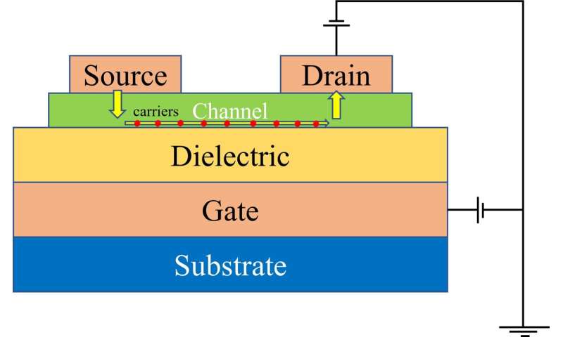
Any valid operable transistor for Complementary Metal-Oxide Semiconductor (CMOS) technology is composed of four main parts: a substrate upon which the components of a semiconductor device are fabricated, a channel that is a path for current to flow, a dielectric that blocks excessive leakage current from the channel to the substrate and enhances device reliability, and three contacts: gate, source and drain that control current flow through the channel.
Ultra-thin transistors and challenges ahead
One of the most pivotal aspects of the effective performance of modern transistors is their capability to minimize power consumption for applications in low-power devices. According to quantum mechanics, the design of a lower-power device requires minimization of leakage current that can be achieved by using thicker layers of dielectrics. A thicker layer of dielectrics with a higher bandgap provides a sufficiently large energy barrier for charge carriers to tunnel. However, using thick layers of traditional bulk dielectrics is in contrast with the device miniaturization outlook.

Why 2D layered dielectrics?
To address this concern, alternative low-dimensional dielectric materials are required for the next generation of ultra-thin low-power CMOS technologies. In this regard, recent developments in the field of two-dimensional (2D) van der Waals (vdW) materials—known as layered materials—have captured great interest for their possible applications in the next generation of CMOS technologies. vdW materials are layered materials whose elemental compositions are connected one to another via a strong covalent bond in the plane, but their layers are weakly held together with the vdW force in the interlayer direction. Therefore, 2D vdW materials are exfoliable to single layers and are ideal candidates to reach the ultimate scaling limit of transistors due to their naturally passivated surfaces.
Although traditional three-dimensional (3D) dielectrics, e.g., HfO2 and Al2O3 provide high-k solutions for silicon-based semiconductor technologies, they cannot be efficiently scaled and therefore deteriorate device performance in 2D vdW channel transistors. Moreover, the covalent bonds in 3D dielectrics may destroy the naturally passivated bonds in a vdW channel material.
In search of 2D layered dielectrics
To tackle the aforementioned challenges, my colleagues and I, led by Professor William Vandenberghe at the University of Texas at Dallas employed the quantum mechanical approach and sophisticated simulation techniques to investigate the dielectric properties of novel 2D vdW dielectric candidates for their application in the nanoelectronics industry. We used Density Functional Theory (DFT) and identified 32 different 2D vdW dielectrics, of which 6 promising dielectric candidates were introduced for n-MOS Field Effect Transistors (FETs). The introduced candidates belong to the family of rare-earth oxyhalides (HoOI, LaOBr, LaOCl, LaOI, SrI2, and YOBr). Our theoretical study and computational modeling explicitly reveal that these introduced 2D dielectrics with a thickness less than 0.8 nm outperform traditional 3D oxide dielectrics such as HfO2 with a thickness of 10 nm.
Starting from a repository of layered materials, 32 possible candidates for suitable vdW dielectric applications are selected. For each material, the in-plane and out-of-plane macroscopic dielectric constants from the first principles are calculated. The calculated in-plane and out-of-plane dielectric constants locate in the range between 2.5 and 98.4.
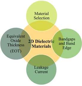
We considered three characteristics while looking for a good vdW layered dielectric candidate: structural stability, small leakage current, and small Equivalent Oxide thickness. These criteria are directly governed by material characteristics. To evaluate the performance of each dialectic material as a gate dielectric in n-MOS applications, we computed the leakage current and the EOT for each candidate. We then computed the leakage current using direct tunneling and thermionic emission equations. The best performing material, monolayer LaOCl, shows immense promise as a gate dielectric, with an EOT of 0.1 nm while maintaining leakage currents much lower than the leakage current specification by the International Roadmap for Devices and Systems (IRDS).

We hope that our research leads to the further exploration of novel 2D layered in device miniaturization and for applications in CMOS technologies, future optoelectronic devices, and the design of functional materials. Fabrication of ultra-thin transistors is now a clear milestone that was set by the electronics industry, and we hope that our research provides a profound theoretical and computational understanding of the new generation of 2D layered dielectric materials suitable for future nanoelectronics devices. For a detailed discussion, you perhaps want to read the full paper by Osanloo et al.
This story is part of Science X Dialog, where researchers can report findings from their published research articles. Visit this page for information about ScienceX Dialog and how to participate.


